


Adjustable repetition frequency
Modular design
TEM00 output
High average power output, up to 30W
Leveraging the extremely small heat-affected zone of "cold processing", it can achieve ultra-fine processing and microstructure production of non-metallic brittle materials in the high-end manufacturing fields, which is widely used in the 3C industry, especially in the key processes of cellphone industry chain. At present, more than 15,000 machines have been launched, leading the market share of similar lasers.
Applications
1. PCB, FPC marking, de-panel, cutting and drilling;
2. Silicon wafer micro-hole and blind hole processing;
3. Solar cell process
4. Silicon wafer scribing
5. Ceramic scribing, cutting and drilling
6. Removal of printing ink, PVD coating
7. Material surface marking
Applications
1. PCB, FPC marking, de-panel, cutting and drilling;
2. Silicon wafer micro-hole and blind hole processing;
3. Solar cell process
4. Silicon wafer scribing
5. Ceramic scribing, cutting and drilling
6. Removal of printing ink, PVD coating
7. Material surface marking
| Model | HL-NS-355-5/10/15 | HL-NS-355-20 |
| Output parameters | ||
| Wavelength | 355nm | |
| Power | 5W/10W/15W | 20W |
| Repetition frequency | 10-200 kHz | 60-400khz |
| Pulse width | 10-100ns | 20-100ns |
| Pulse stability | <3%rms,1σ | <3%rms,1σ |
| Beam parameters | ||
| Spatial pattern | TEM00 | |
| M2 | <1.3 | |
| Polarization ratio | 100:1 (horizontal) | |
| Spot diameter | 1.1 mm ±0.1mm | 1.4mm ±0.2mm |
| Divergence full angle | <2 mrad | |
| Spot symmetry | >90% | |
| Beam pointing | <± 25 µrad/°C | |
| Working conditions/requirements | ||
| Power supply | 100-240V,50 -60Hz | |
| Ready time | Standby to ready<10 minutes; Cold start to ready<30 minutes | |
| Temperature range | Working: 18~35°C; Non-working: 0~50°C | |
| Humidity | 10—90%, no condensation | |
| Cooling requirements | Water cooling, chiller accuracy ±0.1°C & flow rate≥6L/min | |
| Overall heat consumption | <1000 W | |
| Size | ||
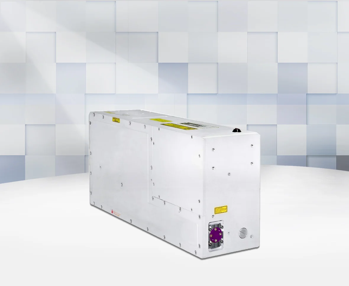
| Size of laser head (L × W × H) | 500mm×230.5mm×132mm | |
| Weight of laser head | 18kg | |
| Size of controller (L × W × H) | 477 mm× 440mm × 177mm | |
| Weight of controller | 21kg | |
Sample
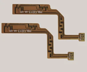
pcb cutting
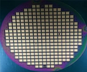
GPP wafer cutting
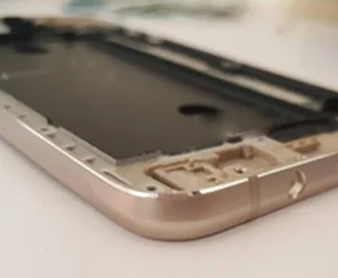
Cellphone middle frame PVD coating removal