


The application of laser annealing
With a super large scale of maturation and scale up of integrated circuit manufacturing technology, new pattern film crystal tube displaying technology and large scale OLED displaying technology, laser annealing has gradually taken place the traditional furnace annealing, thermal annealing, peak annealing and flash annealing then become the new generation mainstream annealing technology.
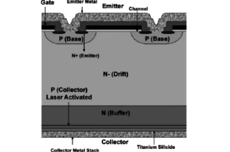
Traditional heating annealing technology involves placing the entire workpiece in a vacuum furnace and annealing it at a certain temperature (300 ° to 1200 ° C) for 10 to 60 minutes, Laser annealing technology has been mainly used to repair semiconductor materials damaged by ion implantation, especially silicon.
The application of laser annealing technology in integrated circuits mainly involves the following three aspects:
(1) annealing the electrodes (source, drain, and gate) of semiconductor devices to form ohmic contacts through metallization;
(2) Annealing the internal connections of integrated circuits;
(3) Perform annealing on 3D structures, such as memorizer, NEMS, etc.