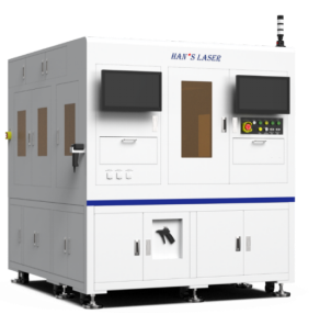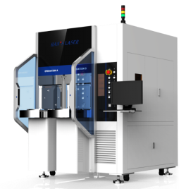





Products
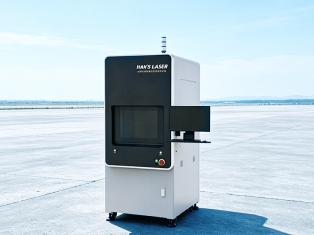

Laser Equipment
General Components
Contact Us
Applications

Han's Laser Solutions
Han's Laser has long prioritized R&D and technological innovation. We now possess world-leading R&D capabilities in laser industry, backed by over 7,400 patents. Leveraging our product strengths, we are continuously expanding full-scenario solutions to empower intelligent manufacturing for various industries worldwide.
View All










Contact Us