


Enabling this setting confirms your approval for cookie implementations throughout the Han’s Laser website, together with the transfer of your personal data to third countries. You may withdraw this authorisation via this interface at any time. Kindly note that all data processing undertaken pursuant to this consent shall remain legally valid prior to your withdrawal.


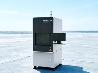
1. Automatic loading and unloading mechanism, high processing efficiency
2. Optional smart vision auto-positioning correction system enables high-precision positioning of chip ceramic substrates.
3. Han’s Laser PMU measurement system with high accuracy, fast testing speed and outstanding consistency.
4. Han’s Laser trimming system supports various trimming path patterns to meet customized customer demands.
5. Capable of trimming parameters including resistance, AC/DC voltage and current.
6. Stable and reliable; trimmed component parameters maintain high stability without drift.
7. Low operation and maintenance cost, high overall efficiency and low power consumption, with built-in protection functions.
Applied to trimming thick-film / thin-film resistors and coated resistor circuits on chip substrates as well as functional trimming of hybrid circuits.