


Enabling this setting confirms your approval for cookie implementations throughout the Han’s Laser website, together with the transfer of your personal data to third countries. You may withdraw this authorisation via this interface at any time. Kindly note that all data processing undertaken pursuant to this consent shall remain legally valid prior to your withdrawal.


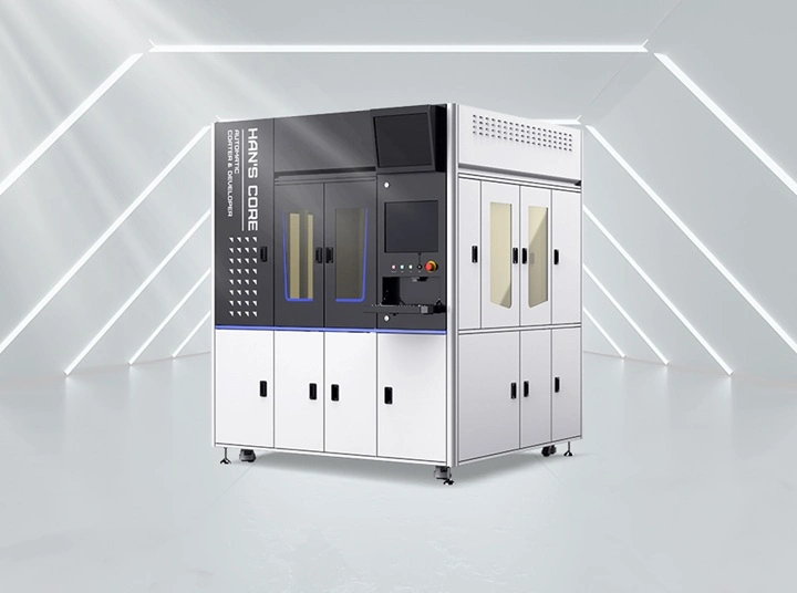
1. Widely applied to photoresist coating and developing processes of silicon, SiC, GaN, GaAs, glass and other materials
2. Supports processes above 0.35 μm, wafer size from 2‑inch to 6‑inch, and is compatible with photoresist ranging from 3‑20000 CP
3. High‑precision control, EtherCAT communication, high‑precision swing arm and wafer‑transfer mechanism
4. Self‑developed software system to support customized requirements
5. Compact footprint, outstanding stability, easy operation and maintenance.
Photoresist coating and developing for Compound‑Semiconductors, Power‑Devices, MEMS, RF‑ICs, LEDs, Research‑based Projects and Optical‑Components
Machine Model | Standard Photoresist Coating and Developing System CD06-XS2C2D1A |
Cassette | 2 & 3CS |
wafer Type | Round Wafers, Square Substrates |
wafer Size(mm) | 50-150 |
Throughput(WPH) | 110 |
Substrate Materials | Si、Glass、Sapphire、GaN、GaAs、SiC、LiTaO3、Li3PO4 |
Processes | g-line、i- line、PI |