


Enabling this setting confirms your approval for cookie implementations throughout the Han’s Laser website, together with the transfer of your personal data to third countries. You may withdraw this authorisation via this interface at any time. Kindly note that all data processing undertaken pursuant to this consent shall remain legally valid prior to your withdrawal.


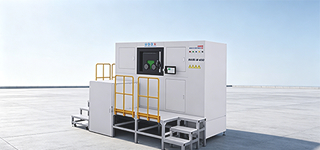
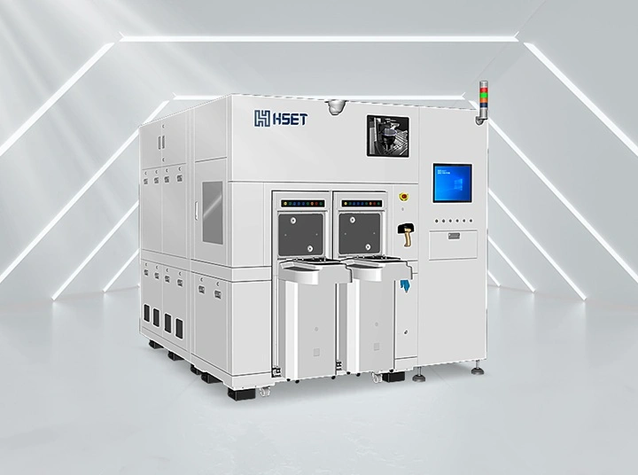
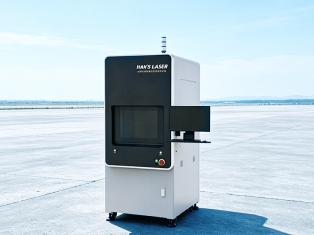
1. Modular design with self‑developed advanced integrated laser technology
2. Highly uniform and stable spot‑energy distribution; compatible with 4‑inch, 6‑inch and 8‑inch thin‑sheet wafers
3. The annealed surface stays uniform and flat, with excellent electrical properties and surface‑morphology
4. Strict control of chamber oxygen content to effectively manage the quantity and distribution of carbon precipitation on the wafer‑surface
5. Equipped with a monitoring‑compensation system for optical‑energy stability and temperature detection on the non‑annealing side
6. Built‑in EFEM wafer‑transfer system. The equipment conforms to SEMI standards and supports SECS‑GEM communication
Anneal the transition metal deposited on the heavily‑doped silicon‑carbide (SiC) surface to form favourable ohmic‑contact.
Machine Model | SiC Laser-Annealing Equipment |
Supported Wafer Sizes | 4inch、6inch、8inch |
Thin‑Wafer Annealing | Supported |
Beam Shaping | Top‑hat Beam |
Beam Uniformity | >95% |
Energy Stability | ≤1% |
Specific‑Contact‑Resistivity | ≤5×10^(-5)Ω.cm² |
Surface Temperature | Annealed‑side >1500℃ Non‑annealed‑side <100 ℃ |
Chamber Oxygen Content | N2/Ar:99.99%,<100ppm @25s |
Motion‑Stage Accuracy | Straightness:±1μm Repositioning Accuracy:±1μm |
Wafer‑Transfer Mode | Automatic Transferring (compatible with wafers or wafer carriers) |