

Enabling this setting confirms your approval for cookie implementations throughout the Han’s Laser website, together with the transfer of your personal data to third countries. You may withdraw this authorisation via this interface at any time. Kindly note that all data processing undertaken pursuant to this consent shall remain legally valid prior to your withdrawal.


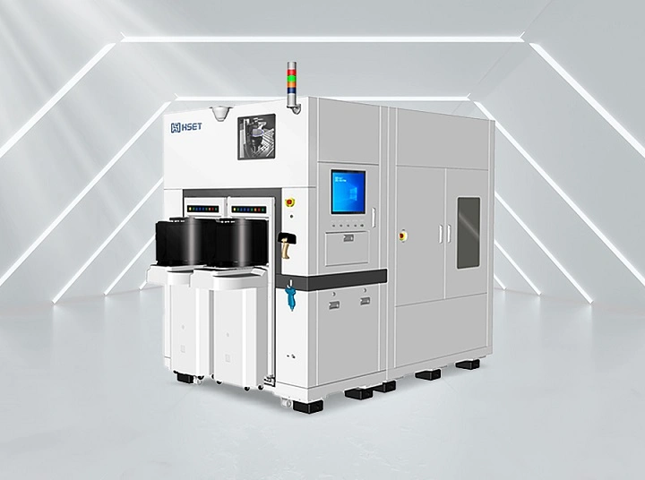
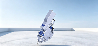
1. The light‑source system developed for the properties of silicon material achieves high‑precision internal modification cutting.
2. Equipped with a far‑infrared back‑penetrating vision system for the back‑side cutting process of silicon wafers.
3. FOUP loading and high‑efficiency wafer transportation by robotic handler.
4. Industrial vision enables fast identification of wafer contour and notch.
5. Fully‑automatic operation for 12‑inch wafers.
6. Complies with SEMI standards and supports SECS‑GEM communication.
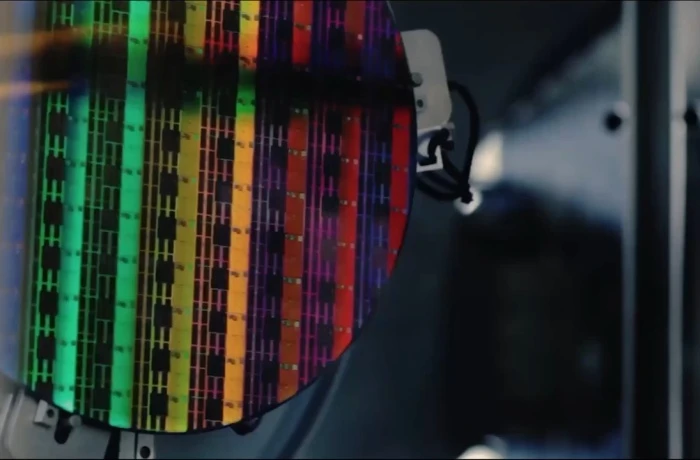
It is mainly adopted for the cutting procedure during the SDBG process of thin‑chip wafers. It supports the cutting of Flash, DRAM and other wafers and is applied to Flash Memory, Memory Controller and other fields.
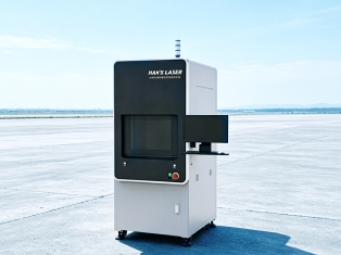
Machine Model | SDBG Process Laser Stealth Dicing Machine |
Wafer Substrate | Si Substrate |
Wafer Size | 12‑inch |
X-Y Travel Range | 600mm×600mm |
Cutting Speed | 400mm-2000mm/s |
Positioning Accuracy | Repositioning accuracy:±1μ Positioning Accuracy:±1μm |
Transmission System | Load port, robot, aligner |
Overall Dimensions (LxWxH) | 2940mm*1600mm*2200mm |