


Enabling this setting confirms your approval for cookie implementations throughout the Han’s Laser website, together with the transfer of your personal data to third countries. You may withdraw this authorisation via this interface at any time. Kindly note that all data processing undertaken pursuant to this consent shall remain legally valid prior to your withdrawal.


1. Combining tank‑soaking treatment with single‑wafer spin‑spraying to improve processing capacity
2. High‑pressure or two‑fluid spraying achieves complete photoresist stripping
3. Substrate workflow: dry‑in, wet‑transfer, dry‑out
4. Photoresist stripper is recovered, circulated, filtered and reused to reduce operating costs
5. Precious‑metal recycling function
Mainly adopted for photoresist‑stripping processes of compound semiconductors, power devices, MEMS, advanced packaging, RF integrated circuits, Micro‑LEDs and optical‑glass substrates
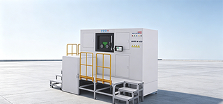
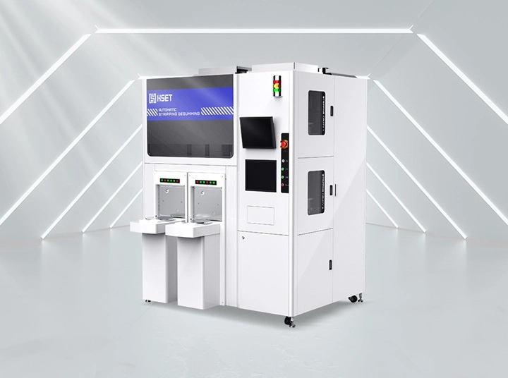
Machine Model | Photoresist‑Stripping Machine LF12-XS3MRS1A |
Cassette Quantity | 2CS&2LP |
Configuration | 1Soak+1Stripper+1Cleaning |
Wafer Type | Round Wafers, Square Wafers |
Wafer Size (mm) | 50-300 |
Throughput(WPH) | 40 |
Chemical Solvents | NMP、DMSO |
Substrate Material | Si、Glass、Sapphire、GaN、GaAs、SiC、LiTaO3、Li3PO4 |
Applicable Processes | Lift-Off、Stripper |
Drying Mode | Spin Dry+N2 Dry |