


Enabling this setting confirms your approval for cookie implementations throughout the Han’s Laser website, together with the transfer of your personal data to third countries. You may withdraw this authorisation via this interface at any time. Kindly note that all data processing undertaken pursuant to this consent shall remain legally valid prior to your withdrawal.


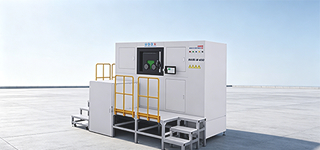
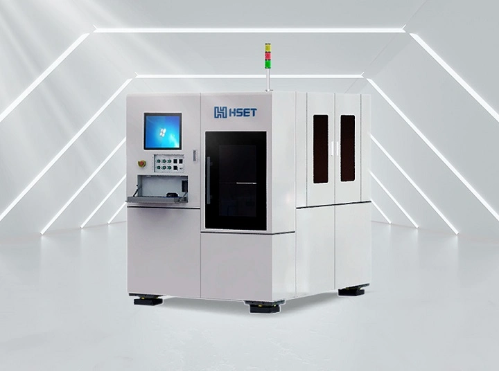
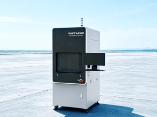
1. Light‑source system developed for the characteristics of LT/LN materials enables high‑precision internal‑modification dicing.
2. High‑speed dicing, superior chipping control, compatible with front‑side and rear‑side dicing processes.
3. Consumable‑free operation and zero‑material‑loss processing.
4. Fully‑automatic operation, compatible with 4‑inch and 6‑inch wafers.
5. Provide systematic solutions, with supporting wafer‑splitting and wafer‑expanding devices.
6. Comply with SEMI standards and support the SECS‑GEM communication protocol.
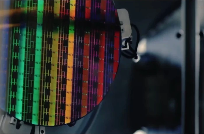
It is adopted for internal‑modification dicing of LT/LN substrate wafers for audio‑video filters, satellite filters, mobile‑communication filters, wireless remote‑control resonators and other components. End‑devices are applied in high‑end‑communication sectors covering mobile phones, two‑way radios, satellite communications and aerospace.
Machine Model | LT/LN Wafer Laser Stealth Dicing System |
Wafer Substrate | LT/LN‑based Substrate |
Wafer Size | 4‑inch, 6‑inch |
Wafer Thickness | 50μm-500μm |
Dicing Speed | 600mm/s-800mm/s |
Positioning Accuracy | Repositioning Accuracy:±1μ Positioning Accuracy:±1μm |
Transport System | Load port, robot, aligner |
Dimensions (LxWxH) | 2070mm×1420mm×2238mm |