

Cookies Consent

Required Cookies (Necessary)
Optional Cookies (statistical analytics cookies)

Enabling this setting confirms your approval for cookie implementations throughout the Han’s Laser website, together with the transfer of your personal data to third countries. You may withdraw this authorisation via this interface at any time. Kindly note that all data processing undertaken pursuant to this consent shall remain legally valid prior to your withdrawal.

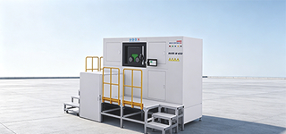
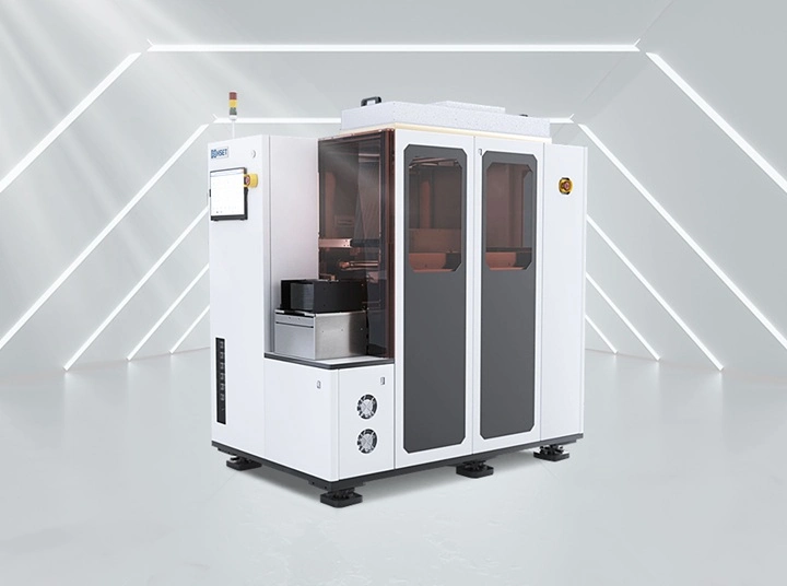
Laser-Ablation Cutting for SiC Wafers DA100-A7 PRO
DA100-A7 PRO

Laser-Ablation Cutting for SiC Wafers

DA100-A7 PRO

Machine Features

1. High‑precision machining for workpieces thinner than 200 μm; fully compatible with wafers under 8‑inch

2. Separation process with one‑step reduction and no‑film‑transfer requirement,

3. Lower CCD with resolution < 1 μm, achieving industry‑leading accuracy

4. Self‑developed multi‑optical‑path system with switchable optical paths for high‑efficiency machining

5. Unattended operation with fully‑automatic loading and unloading

6. Equipped with automatic adhesive coating and cleaning functions


Applications

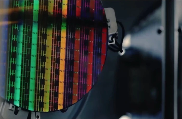
Laser‑surface‑ablation cutting for third‑generation‑semiconductor SiC wafers. It applies to radio‑frequency devices, power‑related components including power diodes, power transistors, thyristors, MOSFETs and IGBTs, as‑well‑as new‑energy vehicles, photovoltaic power generation, smart power grids, rail transit and radio‑frequency communications industries.


Semiconductor Industry
Top