


Enabling this setting confirms your approval for cookie implementations throughout the Han’s Laser website, together with the transfer of your personal data to third countries. You may withdraw this authorisation via this interface at any time. Kindly note that all data processing undertaken pursuant to this consent shall remain legally valid prior to your withdrawal.


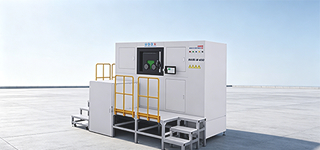
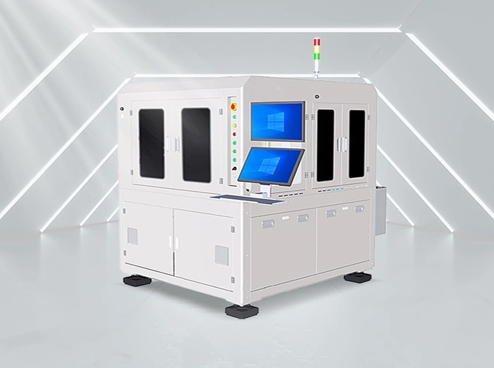
1. Fully‑automatic loading and unloading; processed by high‑speed rotary motor with an hourly output up to 8,000 pieces
2. 24 horizontally‑mounted nozzles with independent control for each unit, and a 4×4 nozzle layout in the vertical direction
3. 4 sorting bins,electrical testing function equipped, multiple‑time bin classification supported
4. High‑precision AOI inspection system
5. Built‑in MES module for full‑lifecycle traceability of product data
The equipment is primarily adopted for wafer‑level testing and post‑packaging test procedures. It evaluates chip performance and quality so that the qualified chips can be proceeded to subsequent packaging workflows. Main inspection items cover electrical indicators and AOI wafer inspection.
Inspected wafers are graded and then placed inside trays for packaging. It serves chip testing for high‑end sectors including industrial, automotive and aerospace industries.
Machine Model | Fully-Automatic Wafer Test-and-Sorting Machine |
Inspection Function | Six‑sided inspection |
Placement Accuracy | ±100um |
Number of Bins | 4 Bins (A / B / C / D) |
Loading Method | Automatic wafer loading |
Unloading Method | Tray, waffle pack, etc. |
Wafer Size | 4", 6", 8", 12" |
Die Size | 0.5x0.5 mm to 30.0x30.0mm |
Die Thickness | 0.1mm up to 1.5 mm |
UPH | 8K-24K |
Testing Function | Supported |
Secondary Bin Sorting | Supported |
Infrared Optical System | Supported |