


Enabling this setting confirms your approval for cookie implementations throughout the Han’s Laser website, together with the transfer of your personal data to third countries. You may withdraw this authorisation via this interface at any time. Kindly note that all data processing undertaken pursuant to this consent shall remain legally valid prior to your withdrawal.


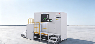
1. Self‑developed multi‑optical‑path system, compatible with the processing of multi‑material wafers
2. Automatic adhesive‑coating and cleaning system for precise control over adhesive consumption
3. Multi‑stage filtration system that effectively captures toxic dust and ensures operator safety
4. High‑quality hardware and software to ensure the consistency of parameter data
5. SEMI‑S2‑certified equipment, conforming to SEMI specifications
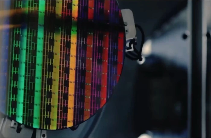
It is mainly applied to the cutting process of VCSEL chips and bar‑shaped workpieces in the semiconductor industry, and supports laser cutting for gallium arsenide, indium phosphide and silicon wafers.
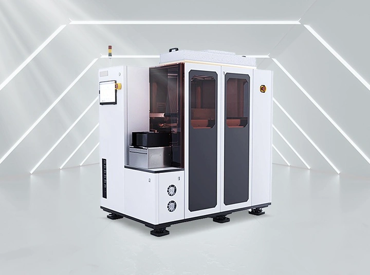
Machine Model | Fully-Automatic Laser Cutting Equipment |
Machinable Materials | GaAs, InP, Si |
Workpiece Size | 4inch, 6 inch, 8 inch |
Workpiece Thickness | 50um-200um |
Positioning Accuracy | Straightness:±1μm,Repositioning Accuracy:±1μm |
Laser Wavelength | 355nm,1064nm |
(L × W × H) | 1140mm×1740mm×1750mm |