


Enabling this setting confirms your approval for cookie implementations throughout the Han’s Laser website, together with the transfer of your personal data to third countries. You may withdraw this authorisation via this interface at any time. Kindly note that all data processing undertaken pursuant to this consent shall remain legally valid prior to your withdrawal.


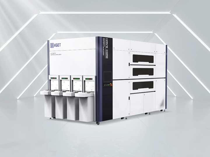
1. Stack‑type high‑throughput structure with a compact footprint
2. Equipped with a multi‑chamber shared photoresist supply system with multi‑stage back‑suction to lower photoresist consumption
3. Optional components including high‑precision hot plate, WEE and AOI units to satisfy higher standard process requirements
4. Modular‑designed core units support flexible configurations and customization
5. Satisfy factory automation demands
6. Achieves inline connection with mainstream lithography tools
Applied to the processing of compound semiconductors, power devices, MEMS, RF integrated circuits and LEDs
Machine Model | Front-end Photoresist Coating and Developing System CD12-XC6C6D1A |
Wafer Cassette Quantity | 4LP |
wafer Type | Round Wafers |
wafer 尺寸(mm) | 200,300 |
Throughput(WPH) | 120 |
Substrate Materials | Si、Glass |
Applicable Processes | PI、I- line、Barc、SOG、SOC、KrF |