


Cookies Consent

Required Cookies (Necessary)
Optional Cookies (statistical analytics cookies)

Enabling this setting confirms your approval for cookie implementations throughout the Han’s Laser website, together with the transfer of your personal data to third countries. You may withdraw this authorisation via this interface at any time. Kindly note that all data processing undertaken pursuant to this consent shall remain legally valid prior to your withdrawal.

Fast! Accurate! Steady! Han's laser creates a powerful brand for semiconductor wafer detecting

Fast! Accurate! Steady! Han's laser creates a powerful brand for semiconductor wafer detecting

Dec 10, 2021
According to SEMI statistics, the market scale of global semiconductor equipment in 2020 is US $59.8 billion, a year-on-year increase of 19%, reaching a record

high of US $71.2 billion. China became the world's leading semiconductor equipment market for the first time. In 2020, the market scale increased by 39% to US

$18.72 billion.


There is a huge market space for semiconductor wafer detecting equipment


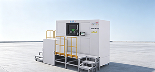
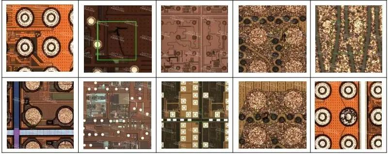
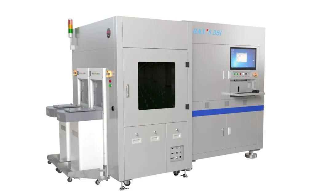
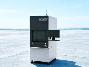
Han’s laser has launched the latest series of detecting products: IFOX series automatic optical wafer detecting equipment. The equipment is suitable for 2D macro

defect detection, dimension measurement and 3D bump measurement of 8-12 inch bare wafers and frame wafers, and can realize multi-dimensional detection of

various characteristics of wafers.


IFOX series automatic optical wafer detecting equipment


Advantages of equipment

1. Fast

● Imaging quality: use the most advanced camera technology to achieve ultra fast scanning with minimal aberration;
● Measurement integration package: Han's laser is the first company to use measurement integration package, which can create a fast measurement scheme in a simple and convenient way;


2. Accurate

● Optical system: the use of independent and advanced large field microscope, equipped with advanced lighting system and real-time focusing technology;
● Defect search: use advanced intelligent defect algorithm to overcome the variation caused by process technology;
● Linear high precision motor, XYZ platform, 100 nm resolution;
● Mechanical structure, 200 nm precision;


3. Steady

● Clean and clean design (the moving platform is on the underside of the wafer);
● Floating base platform reduces the impact of equipment vibration.


Top